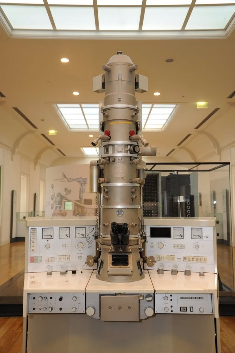
57 YEARS OF #PHOTOVOLTAICS IN ITALY I hope I will be forgiven a small indulgence, but this is one of those events that happen only once in a lifetime, and since it's about MY life, I want to celebrate it and, in this social media age, what better celebration than to share it with my online friends? To make a long story short, exactly 57 years ago, in September 1969, I started working at the Transmission Electron Microscopy Laboratory of the Physics Institute in Bologna. The laboratory director was Prof. Ugo Valdrè, the undisputed father of electron microscopy in Italy. Under his direction, I began working on the preparation of silicon samples to enable the first high-definition observations of the lattice structure of silicon and its related defects. Then many years went by, during which I moved to the CNR, I saw new models of transmission and scanning electron microscopes being developed, always continuing to work on the characterization of materials for the production of photovoltaic cells. In that laboratory, we produced the first solar cells made in Italy and the first photovoltaic panel with an incredibly high efficiency at that time of 12%. These were exciting years, full of beautiful experiences, many small discoveries, and above all, a lot of tedious routine work that allows all those who work with silicon today to deeply understand this material and create increasingly perfect and high-performance products. Well, that's just it, but 57 years have passed, and since at my age, migrating from earthly life to the cloud is instantaneous, I will bore you annually and will stop (for reasons beyond my control) only after I have (reluctantly) completed my migration to the cloud. 😉 ------------------------------------ The larger photo above was taken with a scanning electron microscope and depicts the anti-reflective surface of a monocrystalline silicon photovoltaic cell. These pyramids were obtained through a chemical treatment with a solution of nitric acid and hydrofluoric acid. For decades, this method had been abandoned in favor of screen-printed films, but it is making a comeback in high-efficiency and bifacial cells. ------------------------------------ The smaller photo at the bottom left is the electron microscope image of a dislocation on a silicon crystal. The "dislocation" is a defect in the lattice structure of silicon due to a shift of the atoms. A practical example is a stack of books where some planes overlap others with a small lateral displacement. Lattice defects reduce the efficiency of cells which, to achieve high efficiency, must be made from silicon with a perfect crystal lattice structure. In this specific case, the lattice shift was also used as a resolution test for the electron microscope that could distinguish two objects spaced just 2.5 Angstroms apart. ------------------------------------ The central photo at the bottom is a reconstruction of the first electron microscope invented and made by the Germans Ernst Ruska and Max Knoll in 1931. It is based on the fact that the resolving power is inversely proportional to the wavelength of the radiation used, which is smaller for an electron beam compared to a photon beam, allowing for several orders of magnitude increase. Anyone working in photovoltaics should know that it is thanks to the electron microscope that it is now possible to produce huge silicon wafers free of defects in the atomic lattice structure, which would greatly reduce the efficiency of the cells. I worked for 11 years with one of these machines first at the Physics Institute of Bologna and then at the LAMEL Laboratory of the National Research Council. ------------------------------------ I worked for 11 years with one of these machines first at the Physics Institute of Bologna and then at the LAMEL Laboratory of the National Research Council; in fact, the last photo at the bottom right is of "my" microscope which I cleaned, polished, and maintained more than a new car. Although it was 1969, as you can see, it was a bit fancier and more efficient than the one in the museum and was equipped with X-ray microanalysis for precise characterization of the chemical composition of materials. It operated at 100 kV, 200,000 magnifications with a resolution of 2.5 Angstroms. It was exactly the model in the photo, SIEMENS Elmiskop 102 #photovoltaics #microscopy #historyofthephotovoltaics #electronmicroscope #LAMEL #SolarEnergy #CNR #photovoltaiccells www.fotovoltaici.info (translated)